15.02.2023Open Position MEP/BEP
Open positions for master thesis projects: QIT / Ishihara Lab

1. Waveguide design and fabrication for efficient delivery & collection of light from NV centers in diamond for quantum biosensing

Nitrogen-vacancy (NV) centers in diamond are very promising biosensors. Our goal is to bring the sensing component of such setups down to chip level and realize an on-chip, portable system to perform high-sensitivity and high-accuracy sensing of bio-samples, such as detection of magnetic footprint of cancerous cells.
To achieve this, we will fabricate a diamond substrate with an array of single NV centers and integrate it with a CMOS chip featuring an array of Single-Photon Avalanche Diodes. These photodetectors will enhance detection sensitivity, speed, and signal-to-noise ratio by efficiently capturing light emitted by individual NV centers in the diamond.
Project Goals:
In bio-sample measurements, however, laser excitation must be carefully controlled in order to prevent sample damage. Therefore, we aim to employ photonic structures to precisely direct excitation light to each NV center.
➢ In this work, you will design, simulate, fabricate and optically test the performance of the fabricated waveguides.

Fig.1 Concept of photonic structure driving the excitation light towards the NV centers of a diamond integrated in a SPAD array chip.
Outcome:
The successful completion of this project will prove to be very valuable in enabling the desired diamond-on-chip quantum biosensor. By the end of this MSc thesis project, we anticipate achieving the following outcomes:
• Design and 3D electromagnetic simulations of different waveguide structures and selection of the one matching our system’s criteria.
• Fabrication of these waveguides. This will be carried out in a cleanroom environment and equip you with substantial fabrication experience.
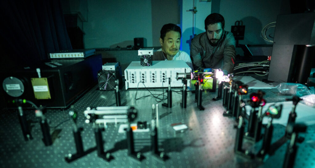
• Characterization of your fabricated waveguides, by making use of optical measurement setups in a lab environment.
For more info, contact:
Ryoichi Ishihara / Yannis Varveris
2. Waveguide-integrated superconducting nanowire single-photon detectors (SNSPD’s)
Efficient detection of single-photon emission is a vital aspect in the design of quantum computers based on color centers in diamond. SNSPD’s are the best candidate for this purpose, showing high detection efficiencies in combination with a low dark-count rate.
Typically, SNSPD’s and qubits are separated from each other, connected by optical fibers. The goal, however, is to integrate all subsystems of the quantum computer on a single chip, which includes the SNSPD’s. On-chip fiber connections are, of course, not practical, so waveguide structures are used instead. SNSPD’s are placed on top of these structures. As the light travels through the waveguides, the photons are absorbed by the nanowire, resulting in a detection event.
Integration of many subsystems on a single chip necessitates footprint reduction of individual components. In an integrated quantum computer, based on defects in diamond, every qubit has multiple SNSPD’s. Reducing the footprint of individual SNSPD’s could potentially significantly reduce the footprint of the whole system.
Project: SNSPD’s on top of optical cavity for footprint reduction
In this project, you will do the following:
- Design of optical waveguide cavity
- Fabrication of the waveguide-integrated SNSPD’s in a cleanroom
- Measurement and characterization of the SNSPD’s
Join the project:
If you are interested to join this project, please contact Salahuddin Nur or Ryoichi Ishihara.
3. Waveguide-integrated superconducting nanowire single-photon detectors (SNSPD’s)
Efficient detection of single-photon emission is a vital aspect in the design of quantum computers based on color centers in diamond. SNSPD’s are the best candidate for this purpose, showing high detection efficiencies in combination with a low dark-count rate.
Typically, SNSPD’s and qubits are separated from each other, connected by optical fibers. The goal, however, is to integrate all subsystems of the quantum computer on a single chip, which includes the SNSPD’s. On-chip fiber connections are, of course, not practical, so waveguide structures are used instead. SNSPD’s are placed on top of these structures. As the light travels through the waveguides, the photons are absorbed by the nanowire, resulting in a detection event.
Integration of many subsystems on a single chip necessitates footprint reduction of individual components. In an integrated quantum computer, based on defects in diamond, every qubit has multiple SNSPD’s. Reducing the footprint of individual SNSPD’s could potentially significantly reduce the footprint of the whole system.
A challenge that arises with integration of the quantum computer subsystems is the change in operation environment for individual components. Color center qubits require biasing with a high static magnetic field. On-chip integration of both qubit and detector requires the SNSPD’s to operate in this magnetic field as well. This requires optimization, since magnetic fields alter the properties of superconducting nanowires.
Project: Investigation of superconductor material suitability for operation in high magnetic fields
In this project, you will do the following:
- Fabrication of SNSPD’s with different superconducting materials in a cleanroom
- Testing of the SNSPD performance in strong magnetic fields.
Join the project:
If you are interested to join this project, please contact Salahuddin Nur or Ryoichi Ishihara.
4. Levitated micro-magnets for quantum sensing
Mechanical oscillators are used in a wide range of applications as force and inertial sensors. The use of a levitated mechanical oscillator based on magnetostatic fields avoids multiple losses and problems other systems have. Combining this with a nitrogen-vacancy (NV) center to create strong spin-mechanical coupling is a promising candidate for quantum sensing, quantum communication and ultra-sensitive magnetometry.
The oscillator consists of a micromagnet contained in a silicon pocket that is levitated with a type II superconductor. The lid of this pocket is a diamond containing NV centers for spin-mechanical coupling. NV centers are fluorescent and when coupled to the magnet the intensity depends on the magnets position. Displacements can thus be precisely determined by measuring the fluorescence of the NV center.
In this research, micro-magnets that range from 1 to 100 μm are levitated with the use of a type II superconductor. The Q-factor, trapping frequencies and coupling strength will be measured for the different sizes of micro-magnets.
Project: Characterization of the levitation properties of micro-magnets of different sizes + coupling to electron spin
In this project, you will do the following:
- Place micro-magnets into small pockets using a pick-and-place system
- Levitate the micro-magnets in a cryostation, and observe the levitation properties with a camera
- Couple the mechanical oscillations of the micromagnet to the spin on an electron in an NV center.
Join the project:
If you are interested to join this project, please contact Salahuddin Nur or Ryoichi Ishihara.
5. Large scale integration of diamond cavity with Sn vacancy
Nanophotonic cavities are a special type of optical resonators which have dimensions in the order of tens to hundreds of nanometers. They are usually implemented with incorporating Bragg reflectors/controlled index variations in the photonic structures. Nanophotonic cavities can strongly confine light/photon, and thus, can significantly enhance photon generation and collection probability from any emitter placed inside the cavity. This unique properties can be used for enhancing the radiative decay rate of a diamond color center emitter, suppressing non-favorable transitions, improving the coherence and spectral purity, spin-photon entanglement generation efficiency, etc. All of these are critical for efficient qubit readout, remote entanglement and large scale diamond based quantum computer, network system implementation. However, fabricating such nanophotonic cavities accurately in diamond and coupling the color center emitters spatially and spectrally with such cavities are highly challenging. Furthermore, a large scale fabrication and high-yield emitter-cavity coupling process has to be developed in order to realize a scalable, on-chip quantum system, where thousands of qubits can be interconnected and entangled efficiently for useful quantum computing.
Tin-vacancy (SnV) centers in diamond is particularly promising for large scale integration of quantum systems because of their charge noise insensitivity due to inversion symmetry, narrow-linewidth and larger ZPL emission (DW factor ~ 0.57), good compatibility of coupling with nanophotonic structures, long spin coherence times at temperatures above 1 K etc.
Hence, developing an integration process for large scale SnV center-cavity coupled system will be a critical step towards the realization of a useful quantum computer and network. In this project, we plan to research and develop efficient, large scale fabrication & coupling techniques for SnV center-cavity systems, which will open the route to scalable, on-chip integration of thousands of qubits in a quantum node/module. Devising a cavity design tolerant to fabrication imperfections and non-optimal emitter positioning can improve the coupling efficiency with simpler fabrication processes. The proposed fabrication processes will allow spatial tuning (placing emitter at field maxima and dipole aligning) of the cavity-emitter system through deterministic cavity fabrication and ion implantation.
[1]. Alison E. Rugar, and et al., Quantum Photonic Interface for Tin-Vacancy Centers in Diamond, Physical Review X, 11, 031021 (2021)
[2]. Maximilian Ruf, and et al., Quantum networks based on color centers in diamond, Journal of Applied Physics 130, 070901 (2021)
[3]. Noel H. Wan*, Tsung-Ju Lu and et al., Large-scale integration of artificial atoms in hybrid photonic circuits, Nature 583, 226–23 (2020).
[4]. Andreas Reiserer, Colloquium : Cavity-enhanced quantum network nodes, Rev. Mod. Phys. 94 041003 (2022)
[5]. Johannes Görlitz, and et al., Spectroscopic investigations of negatively charged tin-vacancy centres in diamond, New J. Phys. 22, 013048 (2020).
[6]. Takayuki Iwasaki, and et al., Tin-Vacancy Quantum Emitters in Diamond, Phys. Rev. Lett. 119, 253601 (2017)
Join the project:
If you are interested to join this project, please contact Salahuddin Nur or Ryoichi Ishihara.
6. Design photonic circuit for cavity enhanced quantum sensor network
Quantum sensors can detect magnetic fields and other physical quantities, with unprecedented spatial resolution and sensitivity. A diamond color center based quantum sensing system, when integrated with photonics and electronics, can provide high sensitivity along with compactness and robustness. Such an on-chip, solid-state system will be very attractive for various fields ranging from biomedical to extreme environment applications [1-3]. The performance of the sensors is expected to be improved by making photonic cavity structure in the diamond connected with carefully designed photonic components, integrating deterministic photon sources, and single-photon detectors etc. Coupling the color center qubits with such a photonic network, the measurement precision of a quantum metrology system can be pushed beyond the standard quantum limit (SQL) by using entangled quantum sensors, which has been demonstrated recently with diamond color center based quantum sensors [4].
A system using levitated mircomagnet combined with the quantum sensor using diamond color center can be used to comprise an entangled quantum sensors network. In this scheme, a small magnetic particle will be levitated in a MEMS cavity in a silicon with a strong magnetic field by superconducting coil and color-center in diamond will be coupled gyroscopically with the motion of the particle. Levitated microobject is in general reported to provide a very high Q factor because of the completely isolated system. Theoretical study of the system operating at a cryogenic temperature of 4K predicts a very high sensitivity (approaching 1013m/s2/Hz1/2). The measurement precision of such a quantum metrology system can be pushed beyond the standard quantum limit (SQL) by using entangled quantum sensors. Recently, this has been demonstrated with diamond color center based quantum sensors [5, 6].
In this project, we design a suitable quantum photonic integrated circuit (QuPIC) for diamond color center spins, with which an on-chip, programmable quantum metrology system can be implemented. and Heisenberg-limited sensing precision can be approached. Furthermore, we will design diamond nanophotonic cavities to couple with levitated micromagnets as a step towards an on-chip, integrated and programmable quantum inertial sensor system. Such an inertial sensor system will enable a performance close to the fundamental quantum limit, compact form factor & robust design – fulfilling very well the stringent requirements for space applications.
[1]. C. L. Degen, and et al., Quantum sensing, Rev. Mod. Phys. 89, 035002 (2017)
[2]. S. B.-Esfahani, and et al., Integrated quantum photonic sensor based on Hong-Ou-Mandel interference, Opt. Express 23, 16008-16023 (2015)
[3] N. Aslam, and et al., Quantum sensors for biomedical applications, Nature Reviews Physics (2023)
[4]. T. Xie, and et al., Beating the standard quantum limit under ambient conditions with solid-state spins, Vol. 7, No. 32, (2021)
[5]. V. Cimini, and Et al., Deep reinforcement learning for quantum multiparameter estimation, Advanced Photonics, Vol. 5, Issue 1, 016005 (2023)
[6]. J. Gieseler, and et al., Single-Spin Magnetomechanics with Levitated Micromagnets, Phys. Rev. Lett. 124, 163604 (2020)
Join the project:
If you are interested to join this project, please contact Salahuddin Nur or Ryoichi Ishihara.
7. Design and fabrication of 1T1R (one transistor one ReRAM) crossbars for neuromorphic computing
Compared with computers, the human brain is incredibly energy efficient. Scientists are therefore drawing on how the brain and its interconnected neurons function for inspiration in designing innovative computing technologies. They foresee that these brain-inspired computing systems, will be more energy efficient than conventional ones, as well as better at performing machine-learning tasks. Artificial neurons which can merge data storage and processing in a single electrical component, that is, the memristor, with good CMOS compatibility, have been anticipated that this will enable higher efficiency as the conventional computers moving data from the processor to the storage consume high energy. We are currently developing new materials for memristors and 1T1R crossbar arrays for Machine learning. One transistor one memristor(s) (1T1R) and Complimentary Resistive Switching devices can solve the chronic sneak path current problem in the existing memristor passive crossbar arrays and thus results in higher reliability, whose research and development contributes to the advancement of the field, to assess the potential applications of neuromorphic technology.
[1] S.I. Yi, J.D. Kendall, R.S. Williams, S. Kumar, Activity-difference training of deep neural networks using memristor crossbars, Nature Electronics, (2022).
[2] M. Prezioso, F. Merrikh-Bayat, B.D. Hoskins, G.C. Adam, K.K. Likharev, D.B. Strukov, Training andoperation of an integrated neuromorphic network based on metal-oxide memristors, Nature, 521 (2015) 61-64.
Join the project:
If you are interested to join this project, please contact Salahuddin Nur or Ryoichi Ishihara.
8. Artificial Neural Network training based on memristors crossbar.
Artificial Neural Networks (ANNs) are a type of machine learning algorithm that are inspired by the structure and function of the human brain. In the field of image classification, ANNs are used to identify and categorize objects or scenes within an image. ANNs are composed of interconnected nodes, or “neurons,” that process and transmit information. Each neuron receives input from multiple other neurons, processes the information, and then transmits the output to other neurons in the network. In this way, ANNs can recognize complex patterns and relationships within data. In the context of image classification, the input to an ANN is typically an array of pixel values that represent an image. The ANN then processes this information, using multiple hidden layers, to produce an output class label that indicates which object or scene is present in the image. To train an ANN for image classification, a large labeled dataset of images is used to teach the network how to recognize different objects or scenes. The network’s output is then compared to the actual class labels and the weights of the connections between neurons are adjusted to minimize the error. ANNs are a powerful tool for image classification tasks, allowing computers to automatically recognize and categorize objects in images with high accuracy.
[1] F. Cai, J.M. Correll, S.H. Lee, Y. Lim, V. Bothra, Z. Zhang, M.P. Flynn, W.D. Lu, A fully integrated reprogrammable memristor–CMOS system for efficient multiply–accumulate operations, Nature Electronics, 2 (2019) 290-299.
Join the project:
If you are interested to join this project, please contact Salahuddin Nur or Ryoichi Ishihara.
9. Integrated optical switch for quantum computer based on spins in diamond
Quantum computer based on spins in diamond connected with photonic circuits is promising for the scalability, their realization poses a host of new engineering challenges.
Specifically, the development of on-chip large-scale photonic circuits for integration with colour centres in diamond is an essential part of the lower stack levels of the quantum computing engines.
Optical switch and other on-chip optical components, such as optical waveguides, will be designed, fabricated in a cleanroom and characterized. Optical switch with MEMS or a novel material will be the candidates for the device. The layer will be integrated with diamond cavity having colour centres and will be controlled by electrical circuits using cryo-CMOS. In the future this will be used for the qubits to be optically coupled and controlled on-chip and inside a cryostat and the fidelity of the basic quantum operation will be characterized.
References
- Ishihara et al., “3D Integration Technology for Quantum Computer based on Diamond Spin Qubits,” 2021 IEEE International Electron Devices Meeting (IEDM), 2021, pp. 14.5.1-14.5.4, doi: 10.1109/ IEDM19574.2021.9720552.
- Seok, N. Quack, S. Han, R. Muller, and M. Wu, “Large-scale broadband digital silicon photonic switches with vertical adiabatic couplers,” Optica 3, 64-70 (2016)
Join the project:
If you are interested to join this project, please contact Salahuddin Nur or Ryoichi Ishihara.
10. Characterization of single photon a valanche diodes and integration with diamond for quantum biosensing
Nitrogen-vacancy (NV) centers in diamond are very promising biosensors. Our goal is to bring the sensing component of such setups down to chip level and realize an on-chip, portable system to perform high-sensitivity and high-accuracy sensing of bio-samples, such as detection of magnetic footprint of cancerous cells.
Project Goals:
To achieve this, we will fabricate a diamond substrate with an array of single NV centers and integrate it with a CMOS chip featuring an array of Single-Photon Avalanche Diodes (SPADs). These photodetectors will enhance detection sensitivity, speed, and signal-to-noise ratio by efficiently capturing light emitted by individual NV centers in the diamond.
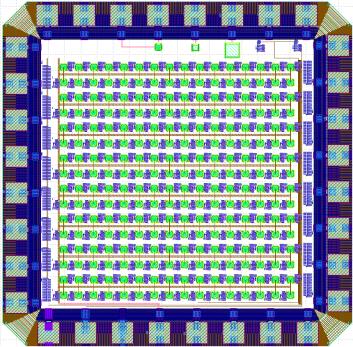
Fig.1 CAD image of the chip containing a 16×16 SPAD array.
This chip has been fabricated using 40 nm CMOS technology (TSMC) and includes on-chip quenching circuits.
➢ In this work, you will characterize the fabricated SPADs, implement readout schemes and finally integrate the chip with the diamond, into the desired compact quantum biosensor.
Outcome:
By the end of this MSc thesis project, we anticipate achieving the following outcomes:
• Characterization of the fabricated SPADs. This includes both electrical and optical measurements, carried out in the EKL lab and our own optical lab.
• Implementation of a readout scheme, using FPGA and other tools, which will enable efficient data collection, from the SPADs to the PC.
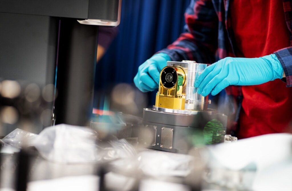
• Integration of the chip containing SPADs with a diamond substrate. In doing so, you will foster scientific advancement and gain valuable experience working in an optical lab whose research focuses on quantum sensing and quantum computing applications.
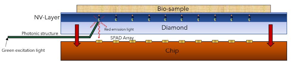
Fig.2 Concept of photonic structure driving the excitation light towards the NV centers of a diamond integrated in a SPAD array chip.
For more info, contact:
Ryoichi Ishihara / Yannis Varveris